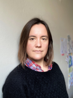
Moïra Hocevar

I am a material scientist, with an expertise in semiconductor nanowire heterostructures. I graduated from INSA de Lyon in France in 2004 as Engineer and later in 2008 with a PhD in Electronics. I have been a postdoc at TU/Delft in The Netherlands until 2012 and then moved back to France to work at CEA Grenoble and Institut Néel. Since 2015, I have been a CNRS research scientist at Institut Néel. I received a "Habilitation à diriger des recherches" from the Université of Grenoble Alpes in 2022. I am interested in difficult crystalline material combinations, for example highly mismatched semiconductors, multi-family semiconductors or dissimilar materials like metals and semiconductors. My research is driven by the challenges encountered at the nanoscale. Defects and surface effects play an important role in nanomaterials. They affect materials, interface and surface quality. It is by their ultimate control that applications based on nano-objects will take off. I grow nanowires for applications in quantum devices, single photon sources, photodetectors, for fundamental research and for the development of novel characterization tools adapted to nano-objects.